Lumped components can easily be incorporated into FEKO in multiple ways. Here is one of those ways that is useful to know.
Each of the solvers — MoM, FEM, and FDTD — will create a load directly onto a port in FEKO. This load is what we will be using to represent the lumped component.
To create a lumped component in FEKO, you simply create a port at the desired location, and then you create a load at the port. These loads can represent a complex circuit, a series circuit, or a parallel circuit — the significance of this being that the load does not have to be a simple reactive-only component.
In addition, the Method of Moments (MoM) solver (Surface Equivalent Principle [SEP] or Volume Equivalence Principle [VEP]) can use a network component to create a more complex load. The network component can be defined manually or in a Touchstone file. Finally, a Spice network can also be included.
How do you incorporate the lumped component into the FEKO model?
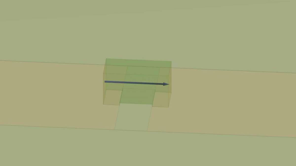
Start by cutting the trace. Once that is done, place a rectangular cuboid on the trace — the specifications of the said rectangular cuboid being defined by the recommended footprint diagram obtained from the vendor of the lumped component in question.
Figure 1 shows an example of this for an 0402 chip. In this example, the Finite Element Mode (FEM) solver is being used.

0.15 mil in height was added to lift the cuboid up off the surface, as shown in Figure 2 for two reasons:
- First, this represents the solder pads.
- Second, it keeps the box representing the chip from touching the surface below, which can be important when using other solvers.

If the lumped component is represented by a solid conductor that is split in the middle with a port placed in between the two halves, then a load can be added onto the port to represent the lumped component.
In the model of the 0402 chip, after adding the feet as seen in Figure 2, the cuboid is given the dielectric of air. The sides are made non-conductive or deleted and the two end faces, which are conductive, are connected with a wire segment. The load is assigned to the wire (see Figure 3), typically in series (see Figure 4).


If the FEM solver is not being used, a network component can be used (see Figure 5). At that point, a Touchstone or a Spice model can be assigned to the port (see Figure 6), providing a more complex model.


Next, the load is edited to add capacitance or inductance, and a resistance is added based on the Spice model or the data sheet for the component, as shown in Figure 7.

Using this technique of adding lumped components directly to your model provides the following advantages:
- By cutting the modeled trace to have the correct gap size needed for the real component, the 3D solver can capture this real effect.
- Since the elements are placed in the model at the correct locations, the effects of the lumped components are more accurately represented.
Some disadvantages are:
- The components may still be too simplified.
- The package itself (like the 0402-sized cuboid) may be adding unacceptable modeling error.
Ultimately, the model is exactly what it is called — namely, a model — and will always need to be validated.

You must be logged in to post a comment.